Semiconductors & Electronic Devices
MOSFET Threshold Voltage: Why It Does Not Mean Fully On
Understand MOSFET threshold voltage, weak inversion, and subthreshold swing, with separate datasheet criteria for threshold and on-resistance.
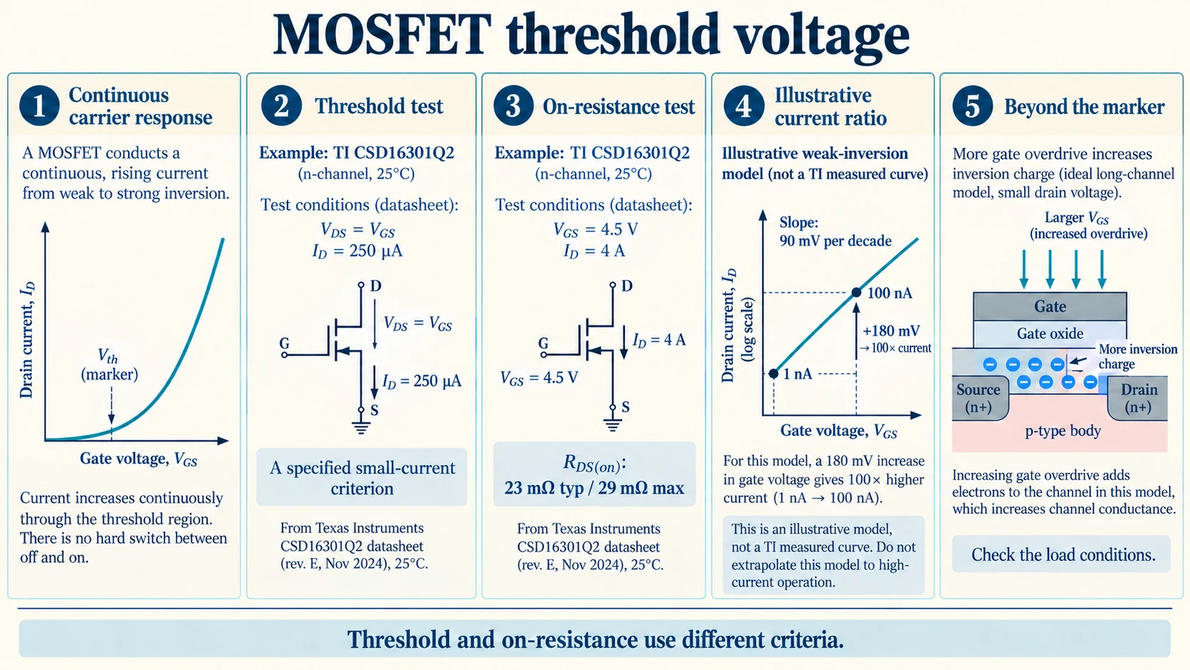
A MOSFET can carry measurable current below its quoted threshold voltage and still have substantial channel resistance slightly above it. The threshold identifies a specified point in a continuous carrier response. How much current flows at that point depends on the device and the conditions used to define the threshold.
Read MOSFET threshold voltage alongside its extraction or test conditions. An on-resistance specification uses its own gate drive and current, with a stated temperature. Keeping both sets of conditions visible prevents a small-current threshold test from being mistaken for a load operating point.
The explanation uses an n-channel device with a p-type body and a bounded long-channel model. It follows the change in surface charge from depletion through inversion, then separates the threshold criterion from additional channel charge. A named datasheet example illustrates distinct test conditions; the model is not a fit to that commercial device.
Clif Fonstad’s MIT 6.012 Fall 2009 notes give the accumulation and inversion model in Lectures 9 and 10. His supplementary MOSFET subthreshold notes derive the diffusion current and the gate-control slope factor. The current-ratio example here is independently calculated from that exponential law, with its slope held fixed. The commercial datasheet example is used only to compare explicit test criteria.
Trace accumulation, depletion, and inversion
Start with a gate separated from a p-type semiconductor by an insulating dielectric. The gate voltage influences the electrostatic potential near the semiconductor surface. Carriers redistribute in response, while the dielectric prevents the gate from acting as a direct ordinary conducting contact to the channel.
For this n-channel example, a gate bias sufficiently below the flat-band voltage attracts holes to the semiconductor surface and produces accumulation. Increasing the gate voltage past the flat-band condition repels holes and creates a depleted region containing negative ionized acceptors. The flat-band reference depends on the gate and semiconductor system, so zero gate voltage is not a universal boundary between these states.
With a sufficiently positive surface potential, electrons become important near the surface. Further gate action can create an inversion layer in which electrons support a channel between source and drain. The carrier concentration does not jump discontinuously at one gate voltage; it changes through the electrostatic and statistical relationships.
An idealized strong-inversion criterion often specifies surface potential relative to the bulk. Practical threshold extraction may instead use a specified current or an extrapolated transfer curve. Each criterion chooses a marker within the model or measurement procedure; the useful load condition needs its own current and gate-drive evidence.
Weak inversion carries diffusion-dominated current
Below a conventional strong-inversion threshold, the surface can still contain electrons. Their population can be small yet sufficient to carry measurable source-to-drain current. Under a bounded long-channel weak-inversion model, the current is dominated by diffusion associated with the source and drain carrier populations.
A common approximate form is ID = Iref exp[(VGS − Vref)/(mUT)] [1 − exp(−VDS/UT)]. Here UT = kT/q is thermal voltage, m is a gate-control slope factor, and the reference quantities specify the model’s scaling.
This expression applies in a suitable weak-inversion regime with stated body and drain conditions and nondegenerate carrier statistics. Lowering gate voltage suppresses the modeled current exponentially. For a finite gate voltage and positive drain bias, the expression retains a finite positive current, although it may fall below an instrument’s resolution.
Interpreting weak inversion requires a declared body condition. The floating-body guide compares transistor currents at matched external voltages after different histories, when retained charge changes the internal body potential. That example explains why terminal voltage labels alone can leave an electrical state unspecified. The exponential diffusion law used here assumes stated body conditions; the linked guide explains a separate source of variation in those conditions.
Other leakage paths can also contribute in real devices. Observing a small off-state current does not establish that all of it follows the simple diffusion model. The measured operating conditions and the current’s dependence on them matter.
Subthreshold swing quantifies a gate-to-current slope
For the exponential model in a region where its other factors remain fixed, define S = dVGS/d(log10ID). This measures how much gate-voltage change produces one decade of drain-current change. The model gives S = mUTln 10.
At a hypothetical temperature of 300 kelvin, UT is about 25.85 millivolts. For m = 1, the corresponding slope is about 59.5 millivolts per decade. A larger m means the gate needs a larger voltage change to produce the same current ratio under this model.
Electrostatic coupling determines how much of a gate-voltage change appears in the relevant semiconductor potential. Within the depletion-based model, the slope factor includes the semiconductor charge response relative to oxide capacitance. A larger slope factor gives a larger gate-voltage change per current decade.
Keep the units and held-fixed quantities visible when interpreting subthreshold swing. The amplifier slew-rate guide derives the time-domain voltage slope required by a sine wave from its amplitude and frequency, then compares it with an amplifier’s specified slope limit. Here the horizontal quantity is gate voltage and the vertical scale is logarithmic drain current. These are different derivatives; a voltage-per-time limit cannot supply a voltage-per-current-decade slope.
The slope is also different from threshold itself. It describes a local change in logarithmic current. A threshold specification identifies a chosen point or extrapolated marker. Two devices can have similar threshold values while exhibiting different current curves and useful on-state behavior.
For an illustrative constant slope of 90 millivolts per decade, increasing the gate voltage by 180 millivolts multiplies the modeled current by one hundred. The absolute current still depends on its starting value and the model’s reference. Raising one nanoampere to one hundred nanoamperes is a large ratio but a small current. This calculation explains why an apparently sharp exponential transition can coexist with a long gap between a detectable-current criterion and a useful load condition. It applies only while the stated exponential model and other bias conditions remain appropriate; it is not an extrapolation through every operating region.
Threshold extraction is not an on-resistance measurement
A datasheet threshold can be defined by the gate-source voltage at which a specified small drain current is reached under stated drain, body, and temperature conditions. Another extraction method can extrapolate a transfer curve. The interpretation must follow the method actually used.
Texas Instruments’ CSD16301Q2 datasheet, revision E from November 2024, provides a concrete example. At 25°C its threshold row uses VDS = VGS and IDS = 250 microamperes. That row lists 0.9 V minimum, 1.1 V typical, and 1.55 V maximum. Its on-resistance rows instead use IDS = 4 A and higher gate voltages.
At VGS = 4.5 V, the same datasheet lists RDS(on) as 23 milliohms typical and 29 milliohms maximum under its stated test. The 250-microampere threshold criterion establishes a different condition from this 4-ampere resistance test. Neither the threshold maximum nor the typical threshold value substitutes for the 4.5 V gate-drive condition.
A threshold range also reflects variation under its test conditions. Treating the largest threshold in that range as the only required gate voltage for a load current ignores the additional charge and conduction conditions. The desired load state must be checked against an applicable operating specification.
For an intended operating point, compare the available gate drive and load current with an applicable resistance specification or transfer measurement at the relevant temperature. A label such as above threshold leaves out the magnitude of channel charge and the resulting voltage drop.
Gate overdrive adds inversion charge in a bounded model
Define gate overdrive as Vov = VGS − Vth. In a simple strong-inversion, long-channel approximation near the source, the inversion charge per unit area is approximately −CoxVov. Raising the gate beyond the threshold marker can therefore add the electron population needed for stronger conduction.
For a small drain-source voltage within the model’s linear regime, the channel conductance is approximately μnCox(W/L)Vov. The corresponding channel resistance scales inversely with overdrive when the other factors are held fixed. A very small positive overdrive does not imply a small resistance.
Actual devices can depart from this approximation through nonuniform channel charge, field-dependent mobility, and resistance outside the ideal channel. The equations explain the role of overdrive. An applicable on-resistance curve or measurement supplies evidence for the commercial operating point.
At larger drain voltage, current need not remain proportional to drain voltage, so one constant resistance may not describe the operating point. Threshold, linear-region conductance, and saturation behavior are distinct parts of a transistor model.
Under the model’s small-drain-voltage assumptions, more overdrive increases channel conductance when mobility, geometry, and oxide capacitance remain fixed. That gives a specific physical step between the threshold marker and stronger conduction. It does not establish the resistance of an unspecified device at an unspecified current.
Temperature and test criteria change the interpretation
Temperature affects thermal voltage and carrier statistics, and it can shift the extracted threshold. Mobility and other current contributions also change. A temperature-driven threshold shift should not be assumed to translate directly into the same direction or size of on-resistance change.
Within the simple weak-inversion expression, increasing T increases UT and changes the gate-voltage slope when the remaining assumptions are retained. Real-device parameters can change simultaneously, so the model does not establish a universal complete transfer curve from temperature alone.
Body bias, drain conditions, and the selected reference current can also affect a threshold measurement. Comparing two quoted thresholds without matching their definitions can confuse a changed test with a changed physical device property.
Retain the transfer data or applicable specification together with the extraction method, temperature, and body and drain biases. Then mark the threshold criterion and the proposed load point separately. This record makes it possible to check whether the same device data actually support the intended operation.
Measurement products do not establish transistor operating points
The Unbranded ZT-703S Electrical Testing instrument, SKU 18623303850, lists oscilloscope, multimeter, and waveform-generator functions with waveform-image storage and export. Those features offer context for a separately specified circuit experiment. Preserve an exported image file as a record of the displayed conditions; its byte representation is not an asserted raw-sample export or a calibrated MOSFET transfer curve.
The Focusrite AMZFCS4I4CR3X Red 4i4 Kit, SKU 1894010824, lists a four-input USB-C audio interface with Air Mode and included Mackie CR3-X monitors. Its powered signal paths offer an electronics context. The listing gives no threshold test or transistor gate-drive requirement for the device model discussed here.
For a selected transistor, copy the complete threshold row and the applicable on-resistance row into the experiment record before choosing a gate drive. Mark the current, drain condition, and temperature beside each row. Compare the intended load point against the row that specifies useful conduction, and keep the threshold criterion visible as a separate measurement.